A Single-Layer Material Could Partially Replace Silicon in Electronics
Silicon can be found in cellphones, computers, and other electronic devices. It is the basic material used to make the semiconductors from which electronics components are made.
Silicon can be found in cellphones, computers, and other electronic devices. It is the basic material used to make the semiconductors from which electronics components are made. But this element, which has been used for decades, has now reached its limits. Researchers at the J. Heyrovský Institute of Physical Chemistry of the CAS have described the properties of chromium triiodide; a 2D material that could partially replace the function of silicon. The important study was published by the scientific journal Physical Review B.
Electronics products are subjected to a constant process of miniaturisation. However, the basic components cannot get much smaller due to the physical properties of silicon. Experts are thus pinning their hopes on advanced 2D materials.
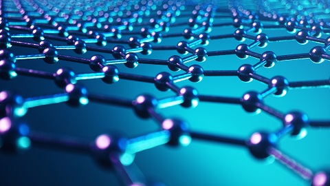
The structure of two-dimensional materials resembles a matrix which is evenly one atom thick. Although hundreds of such single-layer materials are thought to exist, their properties are still not well understood. In fact, it was only 15 years ago that the first of these, graphene, was discovered. “There is a whole family of them. Besides graphene, which is a semimetal, it also includes insulators, semiconductors, superconductors, and magnets,” says Martin Kalbáč from the J. Heyrovský Institute of Physical Chemistry of the CAS.

Representation of the structure of a typical 2D material with the thickness of one atom.
Kalbáč and his colleagues focused their research on chromium triiodide, a material with the chemical formula CrI3. Its structure consists of a single layer of chromium and iodine atoms with a thickness of approximately one nanometre. The aim of the experiments was to reveal how the material would behave under different pressure and temperature conditions. “We subjected the crystal to high pressure of 20 gigapascals or more and monitored the changes in its magnetic state with a spectrometer,” Haider Golam from the same institute explains the experiment.
New and unexpected properties
The team discovered that at a pressure of up to 22 gigapascals, the material behaves like a so-called ferromagnet. It undergoes spontaneous magnetisation, where the spins of all its electrons orient themselves in one direction. Conversely, at pressures above 30 gigapascals, the material begins to exhibit the properties of an antiferromagnet. Here, the spins arrange themselves in opposite directions and the material exhibits almost no external magnetism.
However, experts were interested in the properties of the crystal after exposing it to low temperatures. Between 22–30 gigapascals, chromium triiodide began to behave like so-called spin glass. “Electron spins here can take on many different arrangements. They are not periodically arranged as in conventional magnets,” adds Jana Kalbáčová Vejpravová from Charles University in Prague. The name ‘spin glass’ comes from the fact that its atomic arrangement resembles the structure of silicon and oxygen in glass.

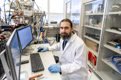
Martin Kalbáč from the J. Heyrovský Institute of Physical Chemistry of the CAS
Faster storage and more data
This property is particularly useful for the production of storage devices, such as computer memories. “Magnetic data storage is a classic way of preserving information,” says Kalbáč, adding that magnetism is principally caused by the spin of electrons in atoms.
Data is stored on magnetic disks by a stable orientation of one magnetic pole being created during the storing. This determines the unit of binary information (1 or 0) that can be read later. “A major advantage of future electronics made from materials such as chromium triiodide is expected to be resistance to external interference and noise.”
Similar technologies are one promising way to increase storage capacity and reduce memory size. Because the 2D material is only a single atom in width, the component can have more storage space. However, according to Kalbáč, this will still not allow the electronics industry to immediately shake its dependence on silicon. “Though it is true that the right combination of 2D materials can provide unique opportunities for designing devices that will have better properties than those built entirely on the basis of silicon.”
Prepared by: Jan Hanáček, Division of External Relations of the CAO of the CAS
Photo: Shutterstock; J. Heyrovský Institute of Physical Chemistry of the CAS
 The text is released for use under the Creative Commons license.
Publication: Anirudha Ghosh, et al., Exotic magnetic and electronic properties of layered
CrI3 single crystals under high pressure, Physical Review B (2022). DOI: 10.1103/PhysRevB.105.L081104.
Original Story Source: Czech Academy of Sciences

 Alerts Sign-up