Solar Energy Collectors Grown from Seeds
Engineers create seeds for growing near-perfect 2D perovskite crystals
HOUSTON – (June 21, 2021) – Rice University engineers have created microscopic seeds for growing remarkably uniform 2D perovskite crystals that are both stable and highly efficient at harvesting electricity from sunlight.
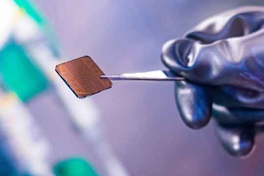 A thin film of 2D halide perovskite crystals of uniform thickness. Rice engineers discovered a self-assembly method for producing the films from "seeds," submicroscopic pieces of 2D crystals that serve as templates. (Photo by Jeff Fitlow/Rice University)
Halide perovskites are organic materials made from abundant, inexpensive ingredients, and Rice's seeded growth method addresses both performance and production issues that have held back halide perovskite photovoltaic technology.
In a study published online in Advanced Materials, chemical engineers from Rice's Brown School of Engineering describe how to make the seeds and use them to grow homogenous thin films, highly sought materials comprised of uniformly thick layers. In laboratory tests, photovoltaic devices made from the films proved both efficient and reliable, a previously problematic combination for devices made from either 3D or 2D perovskites.
"We've come up with a method where you can really tailor the properties of the macroscopic films by first tailoring what you put into solution," said study co-author Aditya Mohite, an associate professor of chemical and biomolecular engineering and of materials science and nanoengineering at Rice. "You can arrive at something that is very homogeneous in its size and properties, and that leads to higher efficiency. We got almost state-of-the-art device efficiency for the 2D case of 17%, and that was without optimization. We think we can improve on that in several ways."
 Aditya Mohite (Photo by Jeff Fitlow/Rice University)
Mohite said achieving homogenous films of 2D perovskites has been a huge challenge in the halide perovskite photovoltaic research community, which has grown tremendously over the past decade.
"Homogeneous films are expected to lead to optoelectronic devices with both high efficiency and technologically relevant stability," he said.
Rice's seed-grown, high-efficiency photovoltaic films proved quite stable, preserving more than 97% of their peak efficiency after 800 hours under illumination without any thermal management. In previous research, 3D halide perovskite photovoltaic devices have been highly efficient but prone to rapid degradation, and 2D devices have lacked efficiency but were highly stable.
 Amanda Marciel (Photo by Jean Lachat)
The Rice study also details the seeded growth process — a method that is within the reach of many labs, said study co-author Amanda Marciel, a William Marsh Rice Trustee Chair and assistant professor of chemical and biomolecular engineering at Rice.
"I think people are going to pick up this paper and say, 'Oh. I'm going to start doing this,'" Marciel said. "It's a really nice processing paper that goes into depth in a way that hasn't really been done before."
The name perovskite refers both to a specific mineral discovered in Russia in 1839 and to any compound with the crystal structure of that mineral. For example, halide perovskites can be made by mixing lead, tin and other metals with bromide or iodide salts. Research interest in halide perovskites skyrocketed after their potential for high-efficiency photovoltaics was demonstrated in 2012.
Mohite, who joined Rice in 2018, has researched halide perovskite photovoltaics for more than five years, especially 2D perovskites — flat, almost atomically thin forms of the material that are more stable than their thicker cousins due to an inherent moisture resistance.
Mohite credited study co-lead author Siraj Sidhik, a Ph.D. student in his lab, with the idea of pursuing seeded growth.
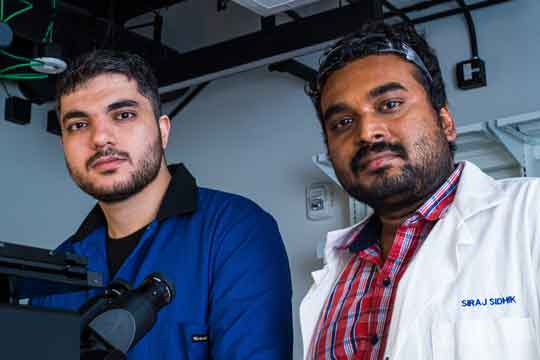 Rice University engineering graduate students Mohammad Samani (left) and Siraj Sidhik discovered a seeded-growth method for creating 2D halide perovskite thin films with layers of uniform thickness. Homogeneous 2D perovskite films have been highly sought and are expected to lead to solar panels and other highly efficient and stable optoelectronic devices. (Photo by Jeff Fitlow/Rice University)
"The idea that a memory or history — a genetic sort of seed — can dictate material properties is a powerful concept in materials science," Mohite said. "A lot of templating works like this. If you want to grow a single crystal of diamond or silicon, for example, you need a seed of a single crystal that can serve as template."
While seeded growth has often been demonstrated for inorganic crystals and other processes, Mohite said this is the first time it's been shown in organic 2D perovskites.
The process for growing 2D perovskite films from seeds is identical in several respects to the classical process of growing such films. In the traditional method, precursor chemicals are measured out like the ingredients in a kitchen — X parts of ingredient A, Y parts of ingredient B, and so on — and these are dissolved in a liquid solvent. The resulting solution is spread onto a flat surface via spin-coating, a widely used technique that relies on centrifugal force to evenly spread liquids across a rapidly spun disk. As the solvent dissolves, the mixed ingredients crystalize in a thin film.
Mohite's group has made 2D perovskite films in this manner for years, and though the films appear perfectly flat to the naked eye, they are uneven at the nanometer scale. In some places, the film may be a single crystal in thickness, and in other places, several crystals thick.
 Rice University chemical engineering graduate student Siraj Sidhik holds a container of 2D perovskite "seeds" (left) and a smaller vial containing a solution of dissolved seeds that can be used to produce thin films for use in highly efficient optoelectronic devices like high efficiency solar panels. (Photo by Jeff Fitlow/Rice University)
"You end up getting something that is completely polydisperse, and when the size changes, the energy landscape changes as well," Mohite said. "What that means for a photovoltaic device is inefficiency, because you lose energy to scattering when charges encounter a barrier before they can reach an electrical contact."
In the seeded growth method, seeds are made by slow-growing a uniform 2D crystal and grinding it into a powder, which is dissolved into solvent instead of the individual precursors. The seeds contain the same ratio of ingredients as the classical recipe, and the resulting solution is spin-coated onto disks exactly as it would be in the original method. The evaporation and crystallization steps are also identical. But the seeded solution yields films with a homogeneous, uniform surface, much like that of the material from which the seeds were ground.
When Sidhik initially succeeded with the approach, it wasn't immediately clear why it produced better films. Fortunately, Mohite's lab adjoins Marciel's, and while she and her student, co-lead author Mohammad Samani, had not previously worked with perovskites, they did have the perfect tool for finding and studying any bits of undissolved seeds that might be templating the homogeneous films.
"We could track that nucleation and growth using light-scattering techniques in my group that we typically use to measure sizes of polymers in solution," Marciel said. "That's how the collaboration came to be. We're neighbors in the lab, and we were talking about this, and I was like, 'Hey, I've got this piece of equipment. Let's see how big these seeds are and if we can track them over time, using the same tools we use in polymer science.'"
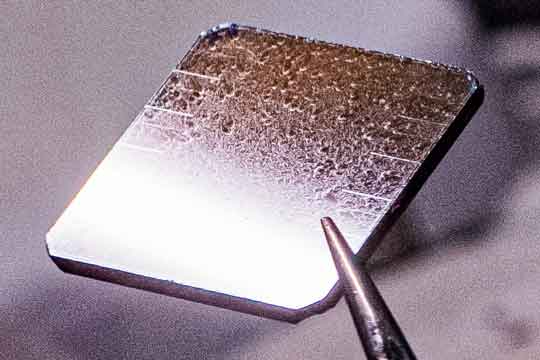 A thin film of 2D halide perovskite crystals that was grown with Rice University's seeded-growth method. The solution processing method yields thin films of remarkably uniform thickness, a highly sought feature that's expected to lead to high-efficiency solar panels and other optoelectronic devices. (Photo by Jeff Fitlow/Rice University)
The tool was dynamic light scattering, a mainstay technique in Marciel's group. It revealed that solutions reached an equilibrium state under certain conditions, allowing a portion of some seeds to remain undissolved in solution.
The research showed those bits of seed retained the "memory" of the perfectly uniform slow-grown crystal from which they were ground, and Samani and Marciel found they could track the nucleation process that would eventually allow the seeds to produce homogeneous thin films.
Mohite said the collaboration produced something that is often attempted and rarely achieved in nanomaterials research — a self-assembly method to make macroscopic materials that live up to the promise of the individual nanoparticles of which they are composed.
"This is really the bane of nanomaterials technology," Mohite said. "At an individual, single element level, you have wonderful properties that are orders of magnitude better than anything else, but when you try to put them together into something macroscopic and useful, like a film, those properties just kind of go away because you cannot make something homogeneous, with just those properties that you want.
"We haven't yet done experiments on other systems, but the success with perovskites begs the question of whether this type of seeded approach might work in other systems as well," he said.
The research was supported by the Department of Energy's (DOE) Office of Energy Efficiency and Renewable Energy, the Academic Institute of France and the Office of Naval Research (N00014-20-1-2725) and made use of DOE facilities at Argonne National Laboratory and Brookhaven National Laboratory
Publication: Siraj Sidhik, et al., Memory Seeds Enable High Structural Phase Purity in 2D Perovskite Films for High-Efficiency Devices, Advanced Materials (2021). DOI: 10.1002/adma.202007176
Original Story Source: Rice University

 Alerts Sign-up